IBM’s 0.7-Nanometer Chip Stacks 100B Transistors, But Defect Risk Remains Unsolved
What You Need to Know
- IBM announced a chip with 100 billion transistors on a 0.7-nanometer node using vertical stacking.
- The “nanostack” design uses staggered layer arrangement, making internal wiring routing substantially easier than competitors.
- New architecture projects 50% better performance and 70% better energy efficiency versus IBM’s 2021 prototype.
- Production could begin within five years, though manufacturing defects and thermal management remain unsolved challenges.
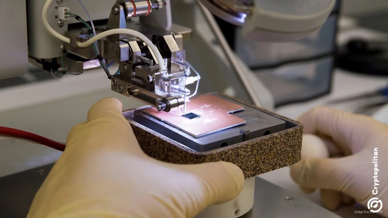
IBM has cracked a barrier that the rest of the semiconductor industry has been circling for years, announcing a chip architecture that fits roughly 100 billion transistors onto a 0.7-nanometer node by stacking them vertically across two bonded silicon wafers. The company projects the design will deliver up to 50% better computing performance and 70% better energy efficiency than its 2021 two-nanometer prototype, with production potentially beginning within five years.
The architecture, which IBM calls a “nanostack” transistor layout, is genuinely novel in one specific way: rather than stacking layers directly on top of each other, IBM uses a staggered arrangement that makes routing internal wiring substantially easier. Qing Cao, a materials science professor at the University of Illinois at Urbana-Champaign, described the demonstration on a full production-grade wafer as “transformative,” and pointed out that Intel, Samsung, TSMC, and Belgian research lab Imec had not landed on the staggered configuration before IBM did. That is a meaningful gap in a field where every major player has enormous R&D budgets and similar access to underlying physics. The catch is that stacking layers compounds manufacturing defects: if either tier fails, the entire chip is lost, and thermal management during fabrication remains an unsolved constraint IBM has not disclosed publicly.
The node name, as IBM itself acknowledges, does not describe a physical measurement. Node naming stopped corresponding to real dimensions decades ago, so “0.7-nanometer” signals capability relative to a theoretical benchmark, not a ruler.
The AI angle is where the commercial pressure becomes legible. IBM says an AI accelerator built on this process could deliver roughly seven times the output of current accelerators, and reported a 40% improvement in SRAM scaling, the fast on-chip memory that AI inference workloads depend on and whose density gains had effectively stalled across recent chip generations. Dan Hutcheson of TechInsights told MIT Technology Review the nanostack approach “puts another ten, fifteen years on the roadmap” for continued transistor scaling, which matters more to hyperscalers and AI hardware buyers than it does to consumer electronics. IBM licenses its process technology rather than manufacturing chips directly, and its current two-nanometer partner is Japan’s Rapidus. No manufacturing partner for the new process has been named yet.
IBM has given itself a ten-year horizon for mainstream adoption, which is an honest timeline but also a long one. The next concrete signal will be whether a foundry partner attaches its name to the process, since without that, the announcement remains a research milestone rather than a product roadmap.


0 Comments